Semiconductor micro-fabrication
Suite of plasma deposition and etching tools for semiconductor processing:
-ICP and RIE etch tools
-PECVD dielectrics deposition
-Metal sputter and evaporation
-Paralyene deposition
-Oxygen plasma ashers
-Rapid thermal annealer
Micro-assembly and systems integration
State-of-the-art micro-assembly tools for hybrid opto-electronic device and systems integration. Including:
-Custom Micro-transfer printing tool with nanoscale accuracy
-Finetech flip-chip bonder
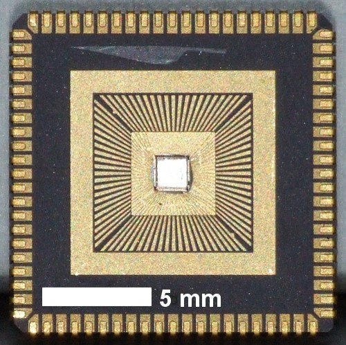
-Wire-bonding toolset
-Clean assembly space for systems manufacturing
Wet chemical processing
Full wet chemistry processing lab with:
-Four wetbench work stations
-Photoresist spinning
-Wet chemical etching and surface treatment
Optical Lithography
UV photo-lithography systems:
-Karl Suss MA6 mask aligner
-Full range of resists and photo-sensitive polymers
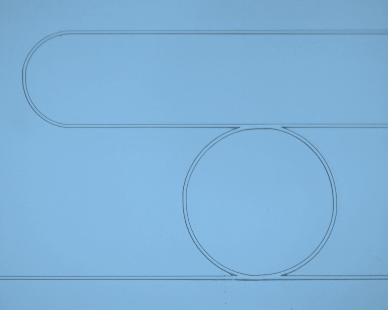
-Fabrication of direct-write waveguide and micro-fluidic devices
Metrology systems
Characterisation and measurement toolset including:
-Atomic Force Microscope
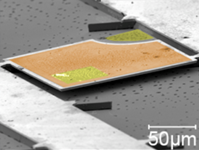
-Scanning Electron Microscope (SEM)
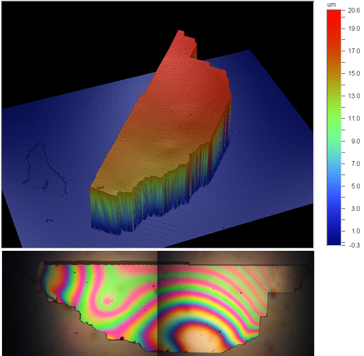
-Optical and stylus surface profileometers
-Electronic probe station
-Thin film interferometry
Access to Cleanroom Facilities
Academic and industrial users can access the TIC cleanroom facilities via a hands-on or serviced basis.
Click here for a current access price list.
Latest news:
